- 您现在的位置:买卖IC网 > Sheet目录1992 > CY28323OXC (Silicon Laboratories Inc)IC CLOCK BROOKDALE GPENT4 48SSOP
CY28323PVC
. Document #: 38-07004 Rev. *B Page Page 16 of 21 of 21
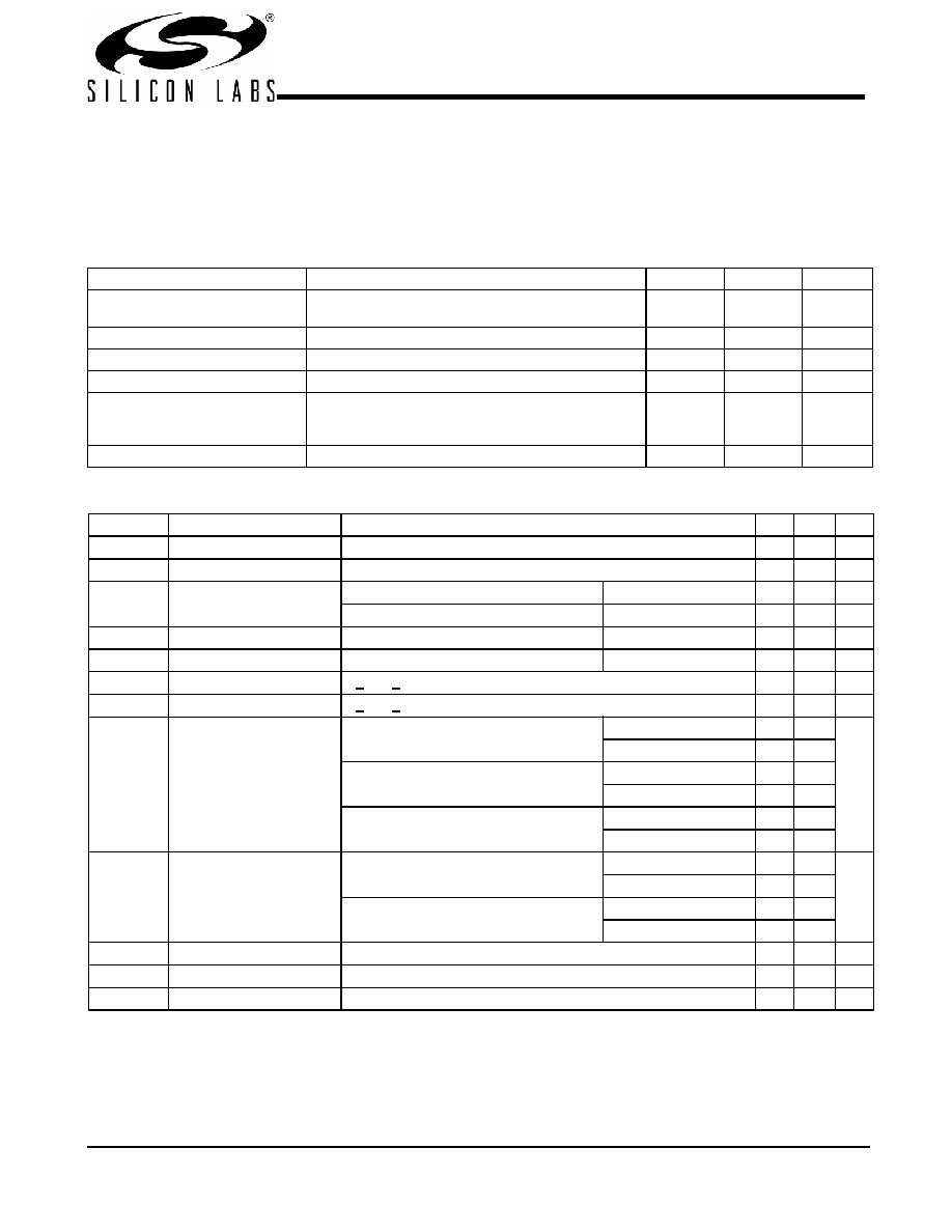
Maximum Ratings
(Above which the useful life may be impaired. For user guide-
lines, not tested.)
Supply Voltage..................................................–0.5 to +7.0V
Input Voltage............................................ –0.5V to VDD + 0.5
Storage Temperature (Non-Condensing) ....–65
C to +150C
Max. Soldering Temperature (10 sec) ....................... +260
C
Junction Temperature................................................ +150
C
Package Power Dissipation............................................... 1
Static Discharge Voltage ........................................................
(per MIL-STD-883, Method 3015) ............................. >2000V
Operating Conditions[2] Over which Electrical Parameters are Guaranteed
Parameter
Description
Min.
Max.
Unit
VDD_REF, VDD_PCI,VDD_CORE,
VDD_3V66, VDD_48 MHz, VDD_CPU,
3.3V Supply Voltages
3.135
3.465
V
TA
Operating Temperature, Ambient
0
70
C
Cin
Input Pin Capacitance
5
pF
CXTAL
XTAL Pin Capacitance
22.5
pF
CL
Max. Capacitive Load on
48MHz, REF
PCICLK, 3V66
20
30
pF
f(REF)
Reference Frequency, Oscillator Nominal Value
14.318
MHz
Electrical Characteristics Over the Operating Range
Parameter
Description
Test Conditions
Min. Max. Unit
VIH
High-level Input Voltage
Except Crystal Pads. Threshold voltage for crystal pads = VDD/2
2.0
V
VIL
Low-level Input Voltage
Except Crystal Pads
0.8
V
VOH
High-level Output Voltage
48MHz, REF, 3V66
IOH = –1 mA
2.4
V
PCI
IOH = –1 mA
2.4
V
VOL
Low-level Output Voltage
48MHz, REF, 3V66
IOL = 1 mA
0.4
V
PCI
IOL = 1 mA
0.55
V
IIH
Input High Current
0 < VIN < VDD
–5
5
mA
IIL
Input Low Current
0 < VIN < VDD
–5
5
mA
IOH
High-level Output Current
CPU
For IOH = 6*IRef Configuration
Type X1, VOH = 0.65V
12.9
mA
Type X1, VOH = 0.74V
14.9
REF, 48 MHz
Type 3, VOH = 1.00V
–29
Type 3, VOH = 3.135V
–23
3V66, PCI
Type 5, VOH = 1.00V
–33
Type 5, VOH = 3.135V
–33
IOL
Low-level Output Current
REF, 48MHz
Type 3, VOL = 1.95V
29
mA
Type 3, VOL = 0.4V
27
3V66, PCI,
Type 5, VOL =1.95 V
30
Type 5, VOL = 0.4V
38
IOZ
Output Leakage Current
Three-state
10
mA
IDD3
3.3V Power Supply Current VDD_CORE/VDD33 = 3.465V, FCPU = 133 MHz
250
mA
IDDPD3
3.3V Shutdown Current
VDD_CORE/VDDQ3 = 3.465V
20
mA
Notes:
2. Multiple Supplies: The voltage on any input or I/O pin cannot exceed the power pin during power-up. Power supply sequencing is NOT required.
发布紧急采购,3分钟左右您将得到回复。
相关PDF资料
CY28354OXC-400
IC BUFF 273MHZ 4DDR DIMM 48SSOP
CY28378OXC
IC CLOCK CK408/TITAN 845 48SSOP
CY284108ZXC
IC CLOCK SERV CK410B 56TSSOP
CY28410OXC-2
IC CLOCK CK410 GRANTSDALE 56SSOP
CY28410OXC
IC CLOCK CK410 GRANTSDALE 56SSOP
CY28411ZXC
IC CLOCK CK410M ALVISO 56TSSOP
CY28442ZXC-2
IC CLOCK ALVISO PENTM 56TSSOP
CY28445LFXC-5
IC CLOCK CALISTOGA CK410M 68QFN
相关代理商/技术参数
CY28323OXCT
功能描述:时钟发生器及支持产品 Brookdale RoHS:否 制造商:Silicon Labs 类型:Clock Generators 最大输入频率:14.318 MHz 最大输出频率:166 MHz 输出端数量:16 占空比 - 最大:55 % 工作电源电压:3.3 V 工作电源电流:1 mA 最大工作温度:+ 85 C 安装风格:SMD/SMT 封装 / 箱体:QFN-56
CY28323PVC
制造商:Rochester Electronics LLC 功能描述:- Bulk
CY28324
制造商:CYPRESS 制造商全称:Cypress Semiconductor 功能描述:FTG for Intel Pentium 4 CPU and Chipsets
CY28324_02
制造商:CYPRESS 制造商全称:Cypress Semiconductor 功能描述:FTG for Intel㈢ Pentium㈢ 4 CPU and Chipsets
CY28324PVC
制造商:Cypress Semiconductor 功能描述:PLL Frequency Generator Dual 48-Pin SSOP 制造商:Rochester Electronics LLC 功能描述:- Bulk
CY28324PVCT
制造商:Rochester Electronics LLC 功能描述:- Tape and Reel
CY28325-2
制造商:CYPRESS 制造商全称:Cypress Semiconductor 功能描述:FTG for VIA Pentium 4 Chipsets
CY28325-3
制造商:SPECTRALINEAR 制造商全称:SPECTRALINEAR 功能描述:FTG for VIA⑩ Pentium 4⑩ Chipsets